Sony increases production capacity for image sensors including back-illuminated and large sized CMOS image sensors


Sony Semiconductor Kyushu Corporation’s Kumamoto Technology Center

Those are good news! I particulary liked this part: “Sony will increase production capacity for mainly large sized “Exmor” used in Digital Single Lens Reflex cameras“!

PRESS RELEASE (via Sony.net):

September 1, 2010, Tokyo, Japan – Sony Corporation (hereafter, “Sony”) today announced that Sony would invest approximately 40 billion yen into Sony Semiconductor Kyushu Corporation’s Kumamoto Technology Center (hereafter, “Kumamoto TEC”), to increase production capacity for “Exmor” and “Exmor R” CMOS image sensors. This investment comprises of an amount previously determined to be invested in the second half of fiscal year 2010, which was included in the forecast for the capital expenditures announced at the earnings announcement for the first quarter ended June 30, 2010, in addition to an amount to be invested in fiscal year 2011.

With this investment, Sony will strengthen its production capacity for image sensors to meet the expected increase in market demand, and continue to solidify its global leadership position in image sensors.

The recent boom in smartphones is creating demand for devices with high image quality and high sensitivity capabilities. Also, the evolution of lighter and more compact Digital Still Cameras as well as improved camera functionality have resulted in an expanding customer segment who own high quality Digital Single Lens Reflex cameras.
These market conditions have led to greater demand for larger image sensors and image sensors with higher image capabilities.

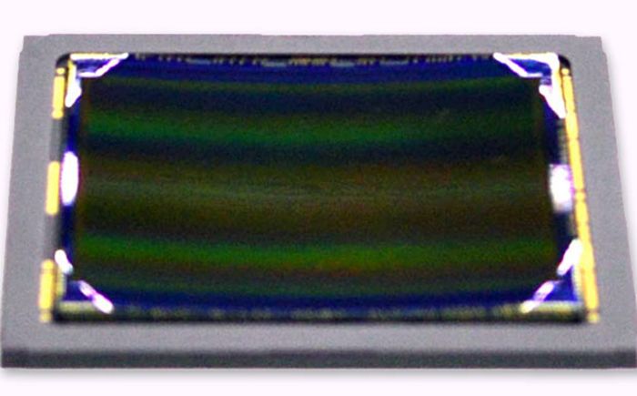
In order to meet these market demands, Sony currently provides two CMOS image sensor models: “Exmor” , which adopts the “Column-Parallel A/D Conversion Technique”, providing each column within the sensor with its own A/D converter to reduce noise; and “Exmor R”, which applies a back-illuminated structure to enhance image characteristics through high sensitivity and reduced noise.

Since 2009, Sony has been mass producing “Exmor R” for Digital Still Cameras and Digital Video Camcorders on wafer lines (with diameter of 200mm) at Sony Semiconductor Kyushu Corporation’s Nagasaki Technology Center. Furthermore, at the end of this year Sony plans to start the mass production of “Exmor R” on wafer lines (with diameter of 300mm) at Kumamoto TEC for mobile phone and compact Digital Still Camera markets.

With the investment announced today, Kumamoto TEC’s CMOS image sensor production capacity will be further increased, and Sony will strengthen its ability to meet the expected market demand for “Exmor R” used in smartphones as well as a wide range of digital imaging products for consumer and professional use, including compact Digital Still Cameras. In addition, Sony will increase production capacity for mainly large sized “Exmor” used in Digital Single Lens Reflex cameras.

Investment Overview

Purpose of investment: Increase production capacity to meet the increasing demand of CMOS image sensors
Investment site: Kumamoto Technology Center, Sony Semiconductor
Kyushu Corporation (Kikuchi-gun, Kumamoto Prefecture)
Investment details: Wafer processing equipment for CMOS image sensor production, etc.
Investment time frame: From the second half of fiscal year 2010 through fiscal year 2011
Investment amount: Approximately 40 billion yen
Production Capacity (Wafer Process/300mm wafers): 25,000 wafers per month
(Before investment this time: 18,500 wafers per month)
-Of them, the capacity for image sensors will be 22,500 wafers per month
(Before investment this time: 16,000 wafers per month)
(Total production capacity of Kumamoto TEC Fab 1 and 2)

Outline of Sony Semiconductor Kyushu Corporation
(1) Head office: 2-3-2 Momochihama, Sawara-ku Fukuoka-shi Japan
(2) Establishment: April 1, 2001
(3) Representative Director (President): Masanori Okayama
(4) Capital: 24.25 billion yen, fully owned by Sony Corporation
(5) Production Bases: Kagoshima, Oita, Nagasaki and Kumamoto
(6) Number of employees: Approximately 9,000 (including contract and temporary employees) as of March 31, 2010
(7) Business Activities: Development, design and production of semiconductors, etc.
Kumamoto Technology Center
(1) Location: 4000-1 Haramizu, Kikuyomachi Kikuchigun, Kumamoto, Japan
(2) Establishment: October 1, 2001
(3) Site area: 256,000-square-meter
(4) Floor area: 195,000-square-meter
(5) Main products:; Image sensors (CCD and CMOS), micro display devices (H-LCD and “SXRD”, etc.)

Thanks R.K. for sending me the link!

Sony TidBits (and new A55v review at Imaging Resource)

[youtube width=”560″ height=”340″]http://www.youtube.com/watch?v=wdMvJBUlEW4[/youtube]

Sony Alpha SLT-A55V review at Imaging Insider!

[shoplink 3058]Sony NEX-VG10[/shoplink] at SonyInsider

Sony Alpha A390 review at Techradar

Sony Cyber-shot DSC-TX7 Review at InfoSync

[shoplink 3003]Sony NEX-5[/shoplink] The ideal Note Pad ? Seen by an AkihabaraNews Fan, 100% subjective and fully assumes it.

Sony Alpha NEX-5 High ISO JPEG Noise preview (Cameralabs)

NEX fisheye lens image samples on PConline

The a560/580 has Mirror Lockup!

After adding the DOF preview Sony also added Mirror Lockup! This has been one of the most requested “features” by Sonyfolk! As you might remember we had a Sony MLU petition (SonyAlphaRumors supported the petition). I guess your pressure did the job and Sony did the great job listening to you!

Source: http://forums.dpreview.com

Official Sony A560/A590 product specifications are available at Sony.net (click here to download the .pdf). Also the A33/A55 manual is available for download

Something else: See the Sony A55v “naked” at CNET Asia ;)

P.S.: Sounds like Kagoo has some A580 cameras in Store